Op Amp Integrator Circuit Applications Circuit Diagram
Op Amp Integrator Circuit Applications Circuit Diagram The practical op-amp integrator differs from basic or ideal integrator circuit in that a resistor RF is used in parallel with the capacitor CF. Also a bias resistor Rb is used. The resistor RF minimizes the problem due to offset voltage and the resistor Rb minimizes the problem due to bias current.

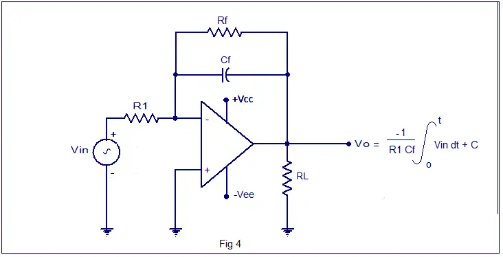
An operational amplifier integrator circuit produces an output voltage which is proportional to the area (amplitude multiplied by time) contained under the waveform. An ideal op-amp integrator uses a capacitor C f , connected between the output and the op-amp inverting input terminal, as shown in the figure below.
How to Build an Integrator Op Amp Circuit Circuit Diagram
An op-amp integrator is a critical part of ADCs, analog computers, and even wave-shaping circuits. While not as common as the voltage follower , comparator , and inverting/non-inverting amplification configurations, the integrator circuit is a great circuit to have in your back pocket. The integrator op amp circuit we will build with an LM741 op amp chip is shown below. Below is the breadboard circuit of the circuit shown above. So, when there is a resistor at the input to the inverting terminal and a resistor and capacitor are in parallel with one side connected to the inverting terminal and the other side to the output, we For the LM358 op-amp based integrator design, let us consider that the input signal amplitude is 100mV and frequency is 1KHz. Let us use single supply voltage 5V for LM358 op-amp. Also let us consider that the output signal should swing around 2.5V. Let the DC gain of an integrator be 10. The LM358 based integrator circuit diagram is shown below.

An operational amplifier (op-amp) integrator circuit is essential in analog signal processing applications such as waveform generation, analog computation, and filtering. In this post, we will walk through the design calculation of a practical op-amp integrator using the LM358 op-amp, with a specified integration time of 25 ms. Additionally, we

Integrator circuit (Rev. B) Circuit Diagram
2. Select a CMOS op amp to minimize the errors from the input bias current. 3. The gain bandwidth product (GBP) of the amplifier will set the upper frequency range of the integrator function. The effectiveness of the integration function is usually reduced starting about one decade away from the amplifier bandwidth. 4.
