Discover the Art of Creating Wearable Electronics Circuit Diagram
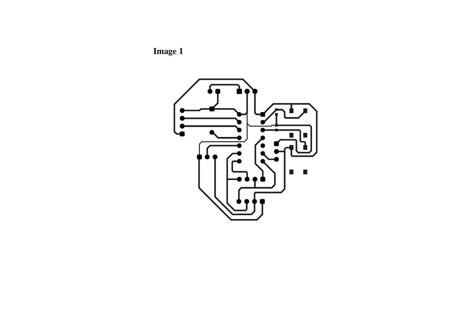
Discover the Art of Creating Wearable Electronics Circuit Diagram Developing a wearable electronic product involves juggling design constraints and compromises in ways that are quite different from more conventional designs. This article discusses the main design tradeoffs for wearable technology products. Putting all the components together will commonly require multiple thin-substrate PCB's that are The explosive growth of wearable technology and ubiquitous computing has revolutionized how we interact with electronic devices. This transformation has brought unique challenges and opportunities in printed circuit board (PCB) design and manufacturing. This comprehensive guide explores the essential aspects of designing PCBs for wearables and ubiquitous computing applications, focusing on

PCB design. The realization of the electronic circuit of a wearable is not limited to the PCB, but includes other materials such as fabric, plastic, rigid-flex boards, and mesh. Unlike traditional rigid PCBs, flex and rigid-flex printed circuit boards are more durable and offer greater resistance to heat, humidity, weather and vibration Solutions from Molex include Quad-Row Connectors that save up to 30% of PCB space, IP67/68/69-rated interconnects for durability and advanced designs to prevent damage during assembly and use. Flexible floating connectors and compact layouts provide design versatility, while robust performance supports seamless integration of advanced features. Wearable Electronics Our industry experience — combined with our state-of-the-art technology and advanced materials — makes us the perfect choice for your next wearable electronics PCB project. We also have extensive experience with the concept of miniaturization and will work with you from the initial design of a project through to the
How to Design a Wearable Technology Product Circuit Diagram
Normally, layer count varies from four to eight layers for wearable devices. Layer structuring is such that if it's an eight layer PCB, it provides enough ground and power plane to sandwich the routing layers. Thus, the ripple effect in crosstalk is kept to a minimum and electromagnetic interference or EMI is significantly reduced.
Printed circuit board (PCB) design is at the center of electronics product development. When creating small gadgets like fitness trackers and other wearable technology devices, it's especially important for design software like Fusion to include detailed PCB capabilities and electronic behavior simulation. In this post, we'll explore the role of PCBs in wearable technology, PCB innovations that have benefited the wearable industry, and how Zuken's CR-8000 software lies at the heart of this revolution. The Role of PCB Design for Wearable Technology. PCB design is the backbone of any electronic device, and wearable technology is no exception.
